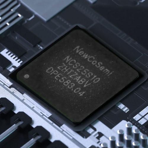
NCS25S10

产品详情

产品描述

High-performance crystal buffer with ultra-low noise floor of -170 dBc/Hz

Low-power clock fanout buffer with additive jitter of 30 fs RMS (typical, 12k to 20M)

Level translation from 3.3V or 2.5V core supply to output supply of 3.3V, 2.5V, 1.8V or 1.5V

Device consists of primary, secondary and crystal inputs which are selectable through input pins.

Clock inputs can accept LVPECL, LVDS, HCSL, SSTL, LVCMOS or LVTTL signals.

Both differential and single-ended inputs are supported with frequencies from DC to 200MHz.

Support either DC or AC-coupled input interface.


产品参数

Crystal frequencies from 8MHz to 50MHz.

Crystal overdrive mode or bypass mode

10 Single-ended LVCMOS output with two independent output supply banks.

Operate up to 200MHz

Low propagation delay of 1ns (typical)

Output skew of 30ps (typical)

Synchronous and glitch-free output enable through input pin

Offered in 32-pin QFN package (5-mm x 5-mm)


Core Supply Voltage(V):2.5V,3.3V

Output Supply Voltage(V):1.5, 1.8, 2.5, 3.3V

Output frequency(Min)(MHz):DC

Output frequency(Max)(MHz):200

Additive Jitter(fs):30

Temperature Range:-40 to 85

Package:32-pin QFN(5mm x 5mm)